From abrasive grit to semiconductor: silicon carbide in power electronics
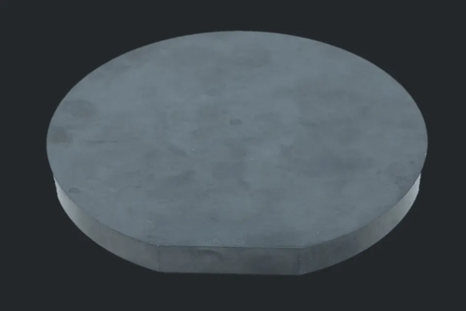
The same compound that saws silicon bricks as green grit has, as a near-perfect single crystal, become one of the key semiconductors for power electronics: in inverters, chargers, rail traction and electric vehicles. Between those two worlds lie orders of magnitude in purity and crystal quality.
Two very different silicon carbides
| SiC as abrasive | SiC as semiconductor | |
|---|---|---|
| Production | Acheson furnace, sand and coke | Single-crystal growth, then epitaxy |
| Form | Crushed, classified grit | Wafers cut from a single crystal |
| Key property | Hardness, angularity | Electronic properties, low defect density |
| Polytype | Mixture, depending on furnace zone | Mostly 4H-SiC |
SiC crystallises in many variants (polytypes) that differ in the stacking sequence of atomic layers. For power devices the hexagonal 4H polytype has prevailed. How the abrasive is made is explained in silicon carbide and the Acheson process.
Why 4H-SiC handles high voltages
Breakdown field
The decisive advantage is the high critical electric field. According to a Mitsubishi Electric lecture series, it is about ten times that of silicon for 4H-SiC (Mitsubishi Electric, SiC Lecture Series 4: "Physical properties of SiC"). As early as 2001, the then head of Infineon's SiC activities cited a bandgap three times, a breakdown field ten times and a thermal conductivity four times that of silicon (EE Times, 14 February 2001).
A figure of merit shows why this matters so much. Baliga's figure of merit (BFOM) is proportional to the inverse of the on-resistance of an ideal unipolar device and grows with the cube of the breakdown field. From the material values, the Mitsubishi source derives that the resistance of unipolar SiC devices can theoretically fall to 1/667 of that of silicon. Because that resistance also rises with the square of the blocking voltage, unipolar silicon devices become impractical in the kilovolt range; with SiC they become feasible.
Thermal conductivity and temperature
Mitsubishi puts the thermal conductivity of SiC at about three times that of silicon, which limits peak temperatures in operation. According to the same source, the material keeps its semiconducting properties up to high temperatures around 800 °C; the practical limit is set by other materials in the device and package.
Thermal conductivity ratios differ between sources (three or four times); they depend on polytype, temperature and the reference value.
Doping and oxide
Unlike many wide-bandgap semiconductors, SiC can be made both n-type and p-type with high carrier concentrations: n-type typically with nitrogen or phosphorus, p-type with aluminium or boron. SiC also grows silicon dioxide as a gate insulator by thermal oxidation, much like silicon. Mitsubishi cites these as key reasons why 4H-SiC has advantages over gallium nitride for power MOSFETs.
The weak spot: the MOS interface
Electron traps form at the interface between SiC and its oxide. They lower channel mobility and contribute to instability and long-term drift of SiC MOSFETs. Trap density depends on the crystal plane: channel mobility is lower on the (0001) plane than on planes perpendicular to it, which is why trench MOSFETs can achieve lower channel resistance than planar ones (Mitsubishi Electric). Oxidation rate also depends strongly on the crystal plane, complicating process control.
Sawing SiC crystals: hard against hard
This closes the circle with the main subject of this site. A SiC single crystal cannot be sawn economically with SiC grit, because the grit is no harder than the workpiece. SiC boules are therefore cut with diamond tools, as diamond wire or as slurry with diamond grit, or by alternative separation methods. The basics of wire sawing still apply (see multi-wire sawing and diamond wire), but cutting times are much longer, and the material value per micrometre of kerf is far higher than for silicon.
A review of thin semiconductor wafer sawing with ultrafine diamond wire notes in general that saw marks a few micrometres deep can noticeably degrade device performance and that finer wires wear and break faster (Ge et al., Materials Science in Semiconductor Processing 203, 2026). With expensive SiC, every micrometre of kerf and every damaged layer that must be ground away weighs especially heavily.
What this means for recycling and the loop
With semiconductor SiC the question shifts. It is not about tonnes of abrasive but about small amounts of a very expensive crystal. What counts most is what is never lost: narrow kerf, shallow damage and little rework by grinding and polishing are the main levers, much as with silicon kerf loss. Substrate materials such as SiC are also explicitly named as a possible innovation dimension for "first-of-a-kind" facilities under the EU Chips Act; see siting wafer and module plants in Europe.
Terms in brief
- Bandgap
- The energy gap between valence and conduction band; a wide bandgap permits high fields and temperatures.
- Critical field (breakdown field)
- The electric field strength at which a material breaks down into avalanche conduction.
- Unipolar device
- A device in which only one type of carrier conducts current, for example a MOSFET or Schottky diode.
- Epitaxy
- Growth of a thin, deliberately doped crystal layer on a substrate wafer.
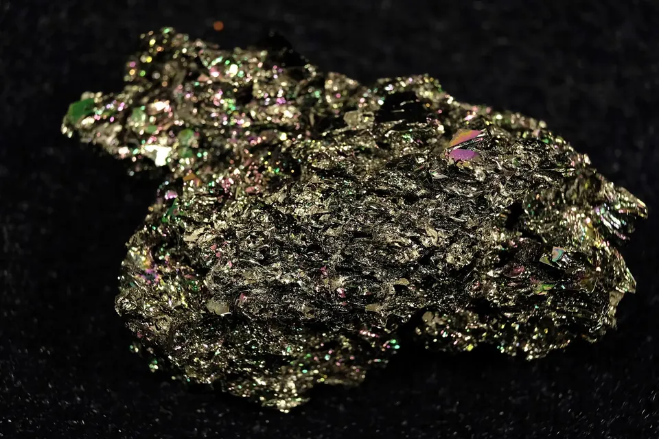 Silicon Carbide
Silicon carbide and the Acheson process
From quartz sand and coke in a resistance furnace: production, green and black SiC, grit and uses.
 Industry & Policy
Site requirements for wafer and chip plants
Cleanroom classes, ultrapure water, grid connection and zoning: what a wafer or chip site must provide.
 Sawing & Wafers
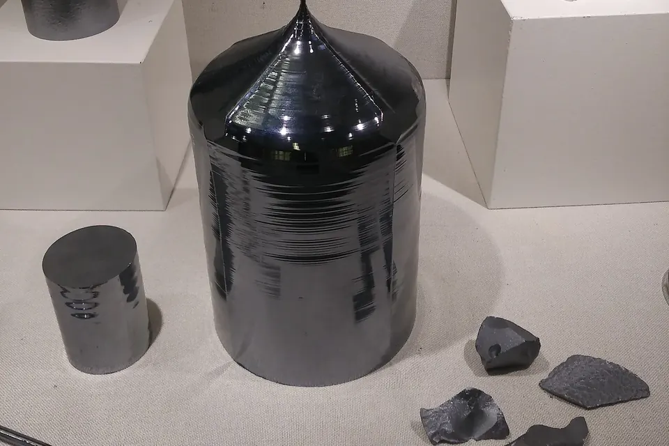
How multi-wire sawing works
Wire web, wire guides and feed: how a silicon ingot becomes hundreds of wafers in a single pass.