Land and buildings for a wafer or chip plant: cleanrooms, ultrapure water, grid connection and zoning
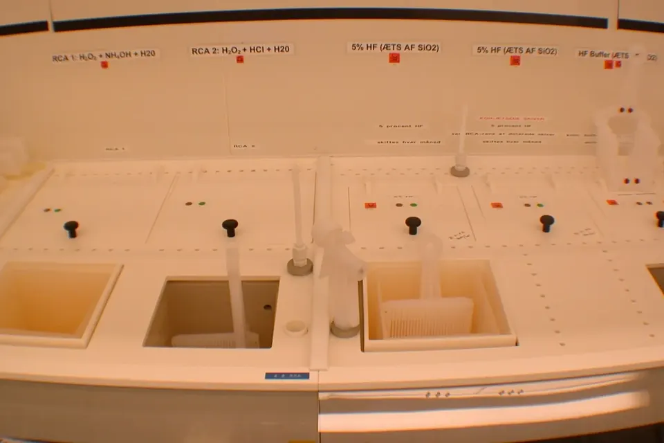
A chip fab or a large wafer plant is not just a factory hall with machines. It is a building engineered around clean air, ultrapure water, uninterrupted power and safe handling of hazardous gases and chemicals. Those requirements narrow the choice of site long before any subsidy is discussed.
Cleanroom space
Semiconductor front-end processing takes place in cleanrooms whose air cleanliness is classified under ISO 14644-1, which defines classes ISO 1 to ISO 9 by the maximum permitted concentration of airborne particles of given sizes. The lower the class number, the cleaner the air. Lithography and other critical steps need the cleanest zones; solar cell lines and back-end packaging generally work with less stringent classes, and module assembly often in controlled but not classified halls.
What this means for the building:
- Air handling on a large scale: filtered air is supplied continuously, often through fan-filter units in the ceiling and a raised perforated floor. The air-handling plant, chillers and exhaust treatment occupy floors or buildings of their own.
- Vibration control: lithography and metrology tools are sensitive to vibration, so fabs need stiff structures and sites away from heavy rail, motorways or quarries, or with a soil and foundation design that compensates.
- Sub-fab and utility levels: pumps, abatement systems and distribution for gases and chemicals usually sit below the cleanroom floor.
- Height and clear spans: the stacking of utility levels, cleanroom and air plenum means building heights and floor loads well above those of an ordinary logistics hall.
Ultrapure water
Wafers are rinsed many times during processing, and the water must be far purer than drinking water: practically free of ions, particles, dissolved organics, bacteria and dissolved gases. The semiconductor industry's reference for ultrapure water quality is SEMI F63, "Guide for Ultrapure Water Used in Semiconductor Processing", published by SEMI Standards. Producing such water from municipal or surface water takes a multi-stage plant (filtration, reverse osmosis, ion exchange, degassing, ultraviolet treatment, ultrafiltration), which itself needs space, energy and chemicals.
For the site, three questions follow:
- Raw water availability: volume and reliability of supply, including in dry years. Water stress is a real constraint in parts of Europe.
- Discharge: treated wastewater contains fluorides, ammonia, acids and other residues depending on processes, and needs a discharge permit and often on-site treatment.
- Reclaim: recycling of rinse water reduces both intake and discharge. The Chips Act guidance explicitly lists reduced use of water and chemicals among innovations that can qualify a fab as "first-of-a-kind" (OJ C/2024/4911).
Fabs or other large water users near protected water bodies come under the Water Framework Directive. Under the Chips Act, security of semiconductor supply may be considered an imperative reason of overriding public interest under that Directive, but only within its existing conditions.
Power supply
A fab or crystal-growing plant draws power around the clock. Two properties matter as much as price:
- Capacity and connection voltage: large plants connect at high voltage, often with their own substation. Grid connection of demand facilities is governed in the EU by the network code on demand connection, Regulation (EU) 2016/1388, with the details set by national grid operators. Lead times for new high-voltage connections can be a decisive factor in site choice, so early enquiries with the transmission or distribution operator are essential.
- Power quality: short voltage dips can stop process tools and scrap wafers in process. SEMI F47 specifies the voltage-sag immunity expected of semiconductor processing equipment; the site still needs a grid with good supply quality, and often on-site buffering for critical loads.
How electricity costs for such loads are measured and compared is covered in industrial electricity prices in the EU.
Gases, chemicals and safety
Fabs and cell lines store and use toxic, flammable and corrosive substances: specialty gases such as silane, phosphine or arsine in chip fabs, hydrogen, hydrofluoric acid, ammonia and solvents. Wafer sawing with water-based coolant can also release hydrogen, as described in the switch to diamond wire. This shapes the site in three ways:
- Major-accident regime: above certain quantities of dangerous substances, an establishment falls under the Seveso III Directive 2012/18/EU, with safety reports, emergency plans and land-use planning that keeps appropriate distances to homes, public buildings and sensitive natural areas.
- Industrial emissions: depending on activities and thresholds, parts of a plant may require a permit under the Industrial Emissions Directive 2010/75/EU, as revised in 2024 by Directive (EU) 2024/1785, with emission limits based on best available techniques.
- Explosion protection and storage: gas yards, bulk chemical storage and tanker access need space and separation distances on the plot.
Zoning and environmental assessment
The plot must be zoned for industrial use that allows these activities, and the zoning must be compatible with the Seveso distances. Large projects typically require an environmental impact assessment under the EIA Directive 2011/92/EU (as amended by Directive 2014/52/EU), covering water, air, noise, traffic, nature and climate. Sites near Natura 2000 areas also need an appropriate assessment under the Habitats Directive.
The Net-Zero Industry Act and the Chips Act speed up these procedures and coordinate them through a single point of contact, but the substantive assessments remain. A brownfield site with existing industrial zoning, grid and water connections can save years compared with a greenfield site, provided soil contamination and old structures are understood.
Space for growth and for the loop
Successful fabs expand, so most site searches look for room for further modules. Space is also needed for the parts of the plant that close loops: water reclaim, chemical recovery, and for a wafering plant, possibly on-site slurry or coolant reprocessing. Planning them in from the start is cheaper than retrofitting.
Checklist
| Topic | Questions for an early site screening |
|---|---|
| Plot | Size including expansion, soil and foundation conditions, vibration sources nearby, contamination |
| Zoning | Industrial zoning, compatibility with Seveso distances, neighbouring land uses |
| Power | Available capacity, voltage level, connection date, supply quality history |
| Water | Raw water source and volume, discharge route and limits, drought risk |
| Hazardous materials | Quantities against Seveso thresholds, gas and chemical logistics |
| Permits | EIA, industrial emissions, water, building; single point of contact; realistic timeline |
| People | Engineering and technician labour market, training institutions |
 Industry & Policy
Siting wafer and module plants in Europe
What the Net-Zero Industry Act and the Chips Act offer a new plant, and the practical criteria for choosing a site.
 Industry & Policy
Industrial electricity prices in the EU
How Eurostat measures electricity prices for non-household consumers, and how to read the bands and price levels.
 Silicon Carbide
SiC in power electronics
Why 4H-SiC suits power semiconductors, and why sawing its very hard crystals is a discipline of its own.