Siting wafer, solar and chip plants in Europe: the Net-Zero Industry Act, the Chips Act and the practical criteria
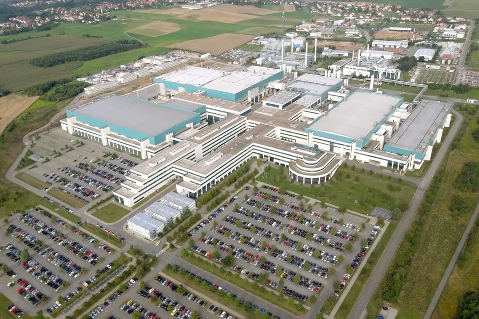
Europe wants more of the solar and semiconductor value chain on its own soil, and since 2023 and 2024 it has two regulations to help: the European Chips Act and the Net-Zero Industry Act. Neither hands out factories. What they change is mostly the permitting process and the framing for public support. Whether a site works still depends on power, water, land, people and logistics.
The starting point
For photovoltaics, the imbalance is well documented. In its special report on solar supply chains, the International Energy Agency found that China's share in all the key manufacturing stages of solar panels, from polysilicon through ingots and wafers to cells and modules, exceeds 80 % (IEA, Solar PV Global Supply Chains, 2022). For semiconductors, the European Commission set itself the aim of doubling the EU's share of global production to 20 % by 2030 in its 2022 Chips Act communication. The European Court of Auditors concluded in 2025 that reaching that target is very unlikely, pointing to the Commission's own projection of about 11.7 % by 2030 (ECA, Special report 12/2025).
Current production and capacity figures for Europe change quickly. The most useful recurring sources are the market reports of SolarPower Europe, the Photovoltaics Report of Fraunhofer ISE and, for chip fabs, the industry data published by SEMI. This article does not quote capacities, because they would be outdated within months.
Which regulation applies to which plant
| Plant type | Main EU framework | Why |
|---|---|---|
| Polysilicon, ingots and wafers, cells and modules for photovoltaics | Net-Zero Industry Act | Solar photovoltaic technology is on the Act's list of net-zero technologies |
| Wafer fabs for chips, including substrate materials such as SiC, and back-end packaging and test | Chips Act | The Act defines semiconductor manufacturing as any stage of production and processing of semiconductor wafers, including substrate materials, front-end and back-end |
| Equipment and key components predominantly used in chip manufacturing | Chips Act | Explicitly included in the "first-of-a-kind" definition |
Both frameworks sit on top of the usual national planning, environmental and industrial-safety law; they speed it up but do not replace it.
The Net-Zero Industry Act
Regulation (EU) 2024/1735 sets a benchmark that EU manufacturing capacity for net-zero technologies should meet at least 40 % of the Union's annual deployment needs by 2030 (European Commission, Net-Zero Industry Act). Its list of technologies includes solar photovoltaic, solar thermal electric and solar thermal technologies. The Act covers final products as well as specific components and machinery primarily used to make them, which is how upstream stages such as wafers and cells come into view.
Permitting time limits
The most concrete benefit is a cap on permit-granting time, counted from the confirmation that the application is complete, including the environmental impact assessment. As summarised by Luxembourg's official business portal (Guichet.lu, net-zero technology manufacturing):
| Project | Annual capacity below 1 GW | Larger, or not measured in GW |
|---|---|---|
| Net-zero technology manufacturing project | 12 months | 18 months |
| Net-zero strategic project | 9 months | 12 months |
Member States may set shorter limits, and the Act allows limited extensions in exceptional cases. Each Member State designates a single point of contact that coordinates the procedure for the applicant.
Strategic projects and acceleration valleys
Projects that meet the selection criteria in Article 13 can be recognised as net-zero strategic projects. According to the Commission, they receive priority status at national level, the shorter time limits above, urgent treatment in judicial and dispute-resolution procedures, and support through the Net-Zero Europe Platform, including advice on financing. Member States can also designate "net-zero acceleration valleys": defined areas where they prepare plans and simplify procedures to cluster net-zero manufacturing.
Demand-side rules
The Act also requires non-price criteria, such as resilience and sustainability, in public procurement and in renewable-energy auctions. For auctions, the Commission states that these criteria must apply to at least 30 % of the volume auctioned per year in each Member State, or to 6 GW per year. For a module or cell maker, that matters as much as permitting, because it shapes whether European products have a market.
The European Chips Act
Regulation (EU) 2023/1781 entered into force on 21 September 2023. It has three pillars: the Chips for Europe Initiative for technological capacity building, a framework for security of supply that attracts manufacturing investment, and a coordination and crisis-response mechanism under the European Semiconductor Board (Commission guidance, OJ C/2024/4911).
"First-of-a-kind" facilities
Under the second pillar, a new or substantially upgraded facility can apply for the status of integrated production facility (IPF) or open EU foundry (OEF) if it is "first-of-a-kind": it must bring an innovation in process or product that is not yet substantively present or committed to be built in the Union. The Commission's guidance lists examples such as a new technology node or substrate material, better energy and environmental performance, reduced use of energy, water or chemicals, or improved recyclability. An IPF is vertically integrated; an OEF offers production capacity to unrelated companies.
What the status brings
- Faster permits: under Article 18, fast-tracking of administrative applications such as environmental assessments and spatial planning, and priority status where national law provides for it. Member States may set up a one-stop shop with a single point of contact.
- Overriding public interest: security of supply of semiconductors may be treated as an imperative reason of overriding public interest under the Habitats Directive and the Water Framework Directive. That is relevant for sites near protected areas or water bodies.
- Pilot lines: priority access to the pilot lines of the Chips for Europe Initiative.
- State aid: the status does not grant money, but the Commission takes the first-of-a-kind dimension into account when assessing aid that a Member State notifies under Article 107(3)(c) TFEU.
Public support beyond the two Acts
Investment aid for clean-technology manufacturing falls under state aid rules. In June 2025 the Commission adopted the Clean Industrial Deal State Aid Framework, which replaced the earlier temporary crisis framework and allows support for net-zero manufacturing capacity, among other things (Net-Zero Navigator: CISAF). Whether, and how much, a given project can receive depends on national schemes and on notification to the Commission.
The practical site criteria
Regulation shortens the path; it does not make an unsuitable site suitable. For wafer, cell, module and chip plants, the recurring criteria are:
- Grid connection: available capacity at a suitable voltage level and a realistic connection date. Crystal growing and chip fabs are large, continuous loads; see site requirements for wafer and chip plants.
- Electricity price and contract options: network charges, taxes and levies differ by country and consumption band, and long-term supply contracts matter; see industrial electricity prices in the EU.
- Water: volume, quality and discharge permits, especially for ultrapure-water-intensive processes.
- Land and zoning: industrial zoning that allows hazardous substances, distance to residential areas and protected sites, room for expansion.
- Skilled labour: process engineers, technicians and maintenance staff, and training capacity nearby.
- Supply chain and logistics: gases, chemicals, glass, frames, wire and grit, transport links and proximity to customers.
- Permitting track record: how quickly the region's authorities have handled comparable projects, and whether an acceleration valley or one-stop shop exists.
None of these can be scored from a desk alone. They need grid operator inquiries, water authority consultations and early contact with the single point of contact, ideally before land is secured.
 Industry & Policy
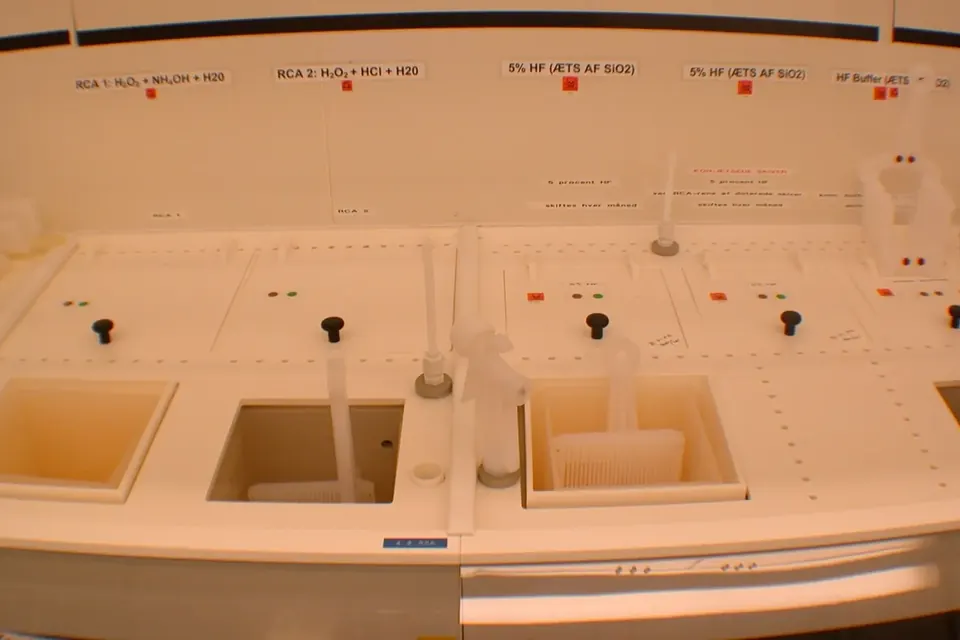
Site requirements for wafer and chip plants
Cleanroom classes, ultrapure water, grid connection and zoning: what a wafer or chip site must provide.
 Industry & Policy
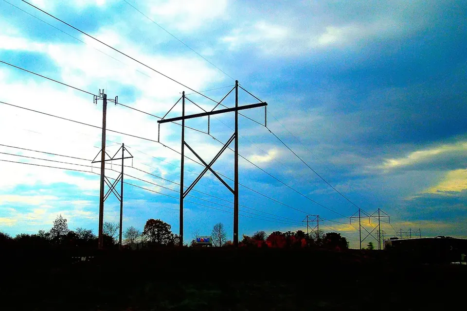
Industrial electricity prices in the EU
How Eurostat measures electricity prices for non-household consumers, and how to read the bands and price levels.
 Industry & Policy
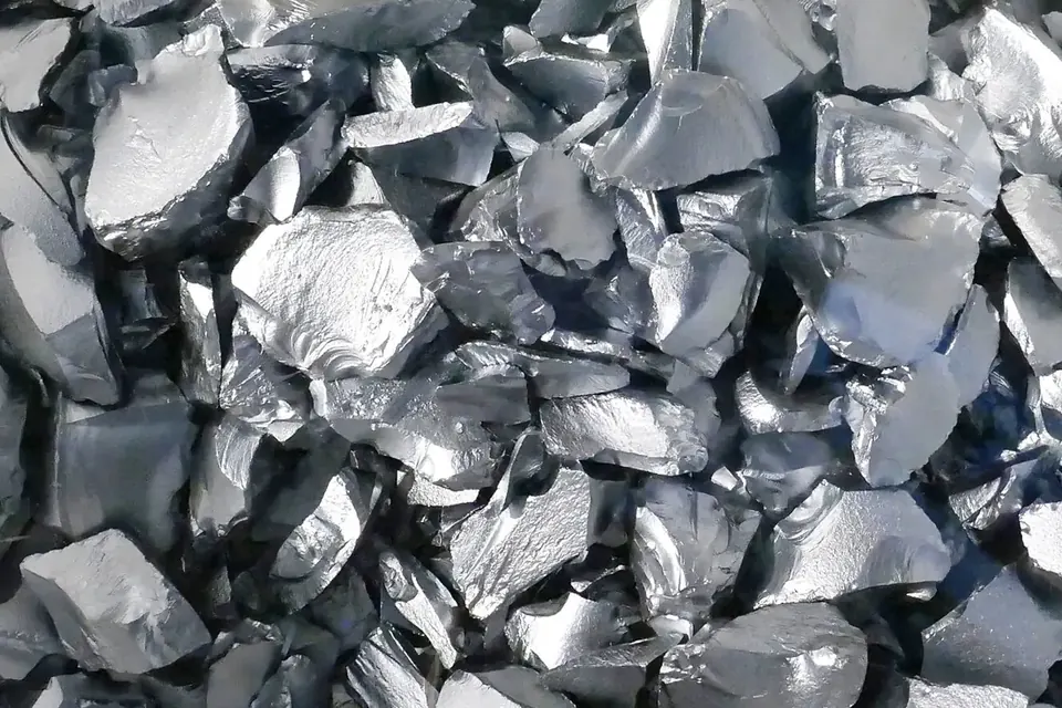
Critical raw materials and silicon
Silicon metal, gallium and germanium under the EU Critical Raw Materials Act: benchmarks, permits and supply risk.