Critical raw materials and silicon: what the EU Critical Raw Materials Act means for wafers and chips
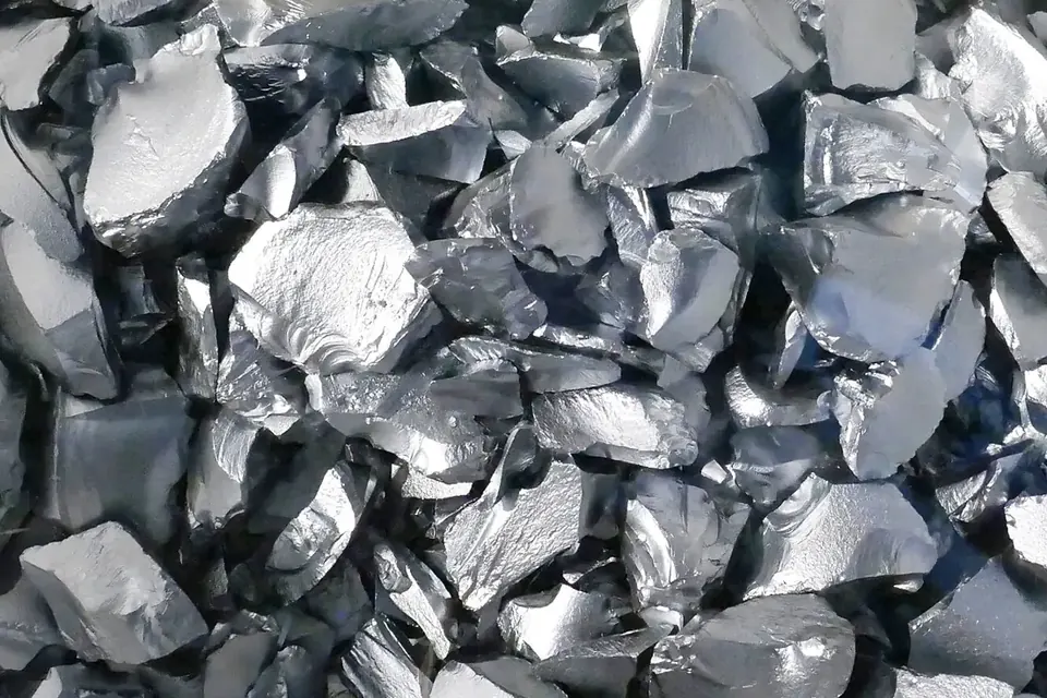
Every solar wafer and almost every chip starts as silicon metal, reduced from quartz in an electric arc furnace and then refined to semiconductor purity. Since 2024, EU law treats silicon metal as a strategic raw material. That label brings benchmarks, faster permits for some projects, and new attention to what is lost and recovered along the way.
The Act in brief
Regulation (EU) 2024/1252, the Critical Raw Materials Act (CRMA), was adopted on 11 April 2024 and entered into force on 23 May 2024. It distinguishes two lists:
- Critical raw materials (34 in the Act): materials of high economic importance with a high supply risk.
- Strategic raw materials (17): critical materials that are also essential for strategic technologies in the green and digital transition, defence and space, with expected demand growth. Every strategic raw material is also on the critical list.
Silicon metal is on the strategic list (Annex I, Section 1), as are gallium and germanium, two elements used in compound semiconductors and optoelectronics (Annexes to the Commission proposal, Council document ST 7568/23 ADD 1; the lists were carried into the adopted text).
The 2030 benchmarks
The Act sets non-binding benchmarks for the EU's capacity along the value chain of strategic raw materials by 2030:
| Benchmark | Share of annual EU consumption of strategic raw materials |
|---|---|
| Extraction in the EU | at least 10 % |
| Processing in the EU | at least 40 % |
| Recycling in the EU | at least 25 % |
| Dependence on a single third country, at any stage of processing | no more than 65 % for each strategic raw material |
For silicon, "processing" covers the production of silicon metal from quartz and its refining; "recycling" covers recovery from scrap and end-of-life products. Both connect directly to this site's subjects: silicon lost as kerf during wafering and silicon in end-of-life solar modules.
Strategic projects and permitting
Projects for extraction, processing or recycling of strategic raw materials can apply to be recognised as strategic projects. For those projects, the Act caps permit-granting at 27 months for extraction and 15 months for processing and recycling, and requires Member States to designate national single points of contact. The Commission selected the first 47 strategic projects inside the EU in March 2025, covering extraction, processing, recycling and substitution in 13 Member States (European Commission, Transition Pathways, 2025). According to reporting on that selection, silicon metal, bismuth and titanium metal were not covered by that first round (electrive, 25 March 2025).
The CRMA and the Net-Zero Industry Act follow the same logic: shorter, predictable procedures and a single contact for projects judged important for supply security. A silicon smelter or a recycling plant for silicon-rich residues would look to the CRMA; a wafer, cell or module plant to the NZIA; a chip fab to the Chips Act.
Why gallium and germanium matter here
Gallium and germanium are by-products of other metal refining and are produced in small volumes, concentrated in few countries. In July 2023 China announced export controls on both, which the EU had already classed as strategic (Euronews, 4 July 2023). For the semiconductor chain this is a reminder that supply risk is not only about silicon: substrates, dopants, process gases and precursors all have their own supply chains.
Obligations for companies
Beyond projects, the Act asks Member States to monitor supply chains and to develop national programmes on circularity, including measures to increase collection and recovery of waste with high critical raw material content. It also asks certain large companies that manufacture strategic technologies to carry out regular supply-risk assessments of their strategic raw materials. Which companies are covered, and how, follows from the Act's articles on risk preparedness; companies should check the text and national implementation rather than rely on summaries.
Where recycling fits for silicon
Silicon is abundant in the Earth's crust as quartz; the bottleneck is the energy-intensive reduction and purification, not geology. Recycling therefore saves less "ore" than energy and processing capacity. Three streams are relevant:
- Kerf from wafering: large in volume, high in purity before contamination, but fine and easily oxidised. Diamond wire made it more recoverable than slurry kerf (Yang et al., Waste Management 84, 2019).
- Broken wafers and off-spec material: cleaner and easier to remelt, but smaller in volume.
- End-of-life modules: growing, but the silicon is bonded in laminates with metals and polymers, and current WEEE targets can be met without recovering it.
For SiC abrasive, which is not on the strategic list, the circular logic is older and simpler: reprocessing sawing slurry saves the electricity of the Acheson furnace and the cost of fresh grit.
What to watch
- Further rounds of strategic project selection, including any covering silicon metal.
- Commission updates of the critical raw materials list, which the Act foresees at regular intervals.
- National circularity programmes and their effect on PV module and production-scrap recycling.
 Industry & Policy
Siting wafer and module plants in Europe
What the Net-Zero Industry Act and the Chips Act offer a new plant, and the practical criteria for choosing a site.
 Industry & Policy
Solar module recycling and the WEEE Directive
How the WEEE Directive covers solar panels, which recovery targets apply and where circularity really stands.
 Slurry & Recovery
Kerf loss and silicon recovery
How much silicon is lost in the cut, why it is hard to win back and which recovery routes research describes.